
Advanced Packaging: The Toll Booth Between GPUs and Memory
The more valuable the chip, the more valuable the package around it becomes.

If you buy a standalone Nvidia H100 GPU today, you’re looking at a price tag between $25,000 and $30,000. But that incredibly expensive piece of silicon is practically a paperweight without one critical piece of infrastructure: High-Bandwidth Memory (HBM)
And the only way to get data from HBM into the GPU at blistering speeds is through advanced packaging.
This is a very lucrative toll booth in the semiconductor industry.
For decades, packaging was a low-margin afterthought. A cheap plastic shell to protect the logic. Today, the advanced packaging market is valued at roughly $40 billion (as of 2024) and is projected to skyrocket to $111 billion by 2034. It has quietly become the definitive bottleneck of the generative AI boom.
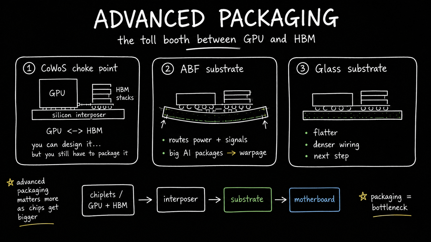
The CoWoS Choke Point
You can design the fastest AI accelerator in the world. But if you can’t package it, you can’t ship it. TSMC’s CoWoS (Chip-on-Wafer-on-Substrate) technology has become the industry’s gold standard. CoWoS places the GPU and HBM side-by-side on a silicon interposer, allowing them to communicate with massive bandwidth over microscopic electrical traces.
This process is so critical that TSMC’s CoWoS capacity literally dictates the pace of global AI infra buildouts. In 2023, TSMC was pumping out a mere 13,000 to 16,000 wafers per month (WPM). By the end of 2024, that ramped up to roughly 40,000 WPM. And for 2025, it’s a staggering 75,000 WPM.
Unsurprisingly, Nvidia commands an estimated 63% of this global supply. To keep up with the overflow, traditional OSATs (Outsourced Semiconductor Assembly and Test) like ASE and Amkor are frantically expanding their own 2.5D and 3D packaging lines to capture the excess demand.
The Unsung Hero: ABF Substrates
Beneath that silicon interposer sits the organic substrate. It’s the unsung hero routing power and data to the server motherboard. Right now, this space is dominated by Ajinomoto Build-up Film (ABF) substrates.
The ABF substrate market was valued at roughly $4.9 billion in 2024 and is expected to reach nearly $10 billion by 2031 (a solid 10% CAGR). It’s an incredibly consolidated niche, with the top five Asian manufacturers controlling 74% of the global market.
But ABF has a fatal flaw: the “warpage wall”. As AI packages swell to massive sizes (some exceeding 100mm x 100mm to accommodate more HBM stacks), the intense heat generated by computing causes the organic ABF resin to warp, cracking the microscopic solder connections.
The Glass Core Revolution
To break the warpage wall, the industry is transitioning to glass. Glass core substrates are the next physical frontier of advanced packaging.
Because glass has a coefficient of thermal expansion that nearly matches silicon, it stays perfectly flat under extreme heat.
It also acts as a superior insulator, supporting sub-2-micrometer wiring. This density is crucial for next-generation architectures like Nvidia’s rumored Rubin, which could require over 50,000 I/O connections to manage its blistering memory bandwidth.
Intel has poured over $1 billion into a glass R&D line in Arizona, pushing to bring glass substrates into high-volume manufacturing between 2026 and 2030. Meanwhile, TSMC recently outlined a 2-to-3-year timeline for its own glass-based CoPoS technology, proving that the entire ecosystem is gearing up for this material shift.
Where do we go from here
Moore’s Law is slowing, making it economically punishing to print massive monolithic chips. The solution is slicing silicon into chiplets and stitching them back together. As the logic itself becomes exponentially more complex, the interposers, ABF films, and glass cores that bind it all together capture progressively more of the margin.
In the AI gold rush, TSMC, Intel, and the OSATs are selling the pickaxes. And they’re building the toll roads too.
If you are getting value from this newsletter, consider subscribing for free and sharing it with 1 infra-curious friend: